- 您现在的位置:买卖IC网 > Sheet目录313 > AT45DB321C-TC (Atmel)IC FLASH 32MBIT 40MHZ 28TSOP
�� �
�
�AT45DB321C�
�Main� Memory� Page� Program� without� Built-in� Erase,� Page� Erase,� Block� Erase,� Main� Memory�
�Page� Program,� and� Auto� Page� Rewrite.�
�Bit� 1� in� the� Status� Register� is� used� to� provide� information� to� the� user� whether� or� not� the� sector�
�protection� has� been� enabled� or� disabled,� either� by� software-controlled� method� or� hardware-con-�
�trolled� method.� A� logic� 1� indicates� that� sector� protection� has� been� enabled� and� logic� 0� indicates�
�that� sector� protection� has� been� disabled.�
�The� device� density� is� indicated� using� bits� 5,� 4,� 3,� and� 2� of� the� status� register.� For� the�
�AT45DB321C,� the� four� bits� are� 1,1,� 0,� 1.� The� decimal� value� of� these� four� binary� bits� does� not�
�equate� to� the� device� density;� the� four� bits� represent� a� combinational� code� relating� to� differing�
�densities� of� DataFlash� devices.� The� device� density� is� not� the� same� as� the� density� code� indicated�
�in� the� JEDEC� device� ID� information.� The� device� density� is� provided� only� for� backward�
�compatibility.�
�The� result� of� the� most� recent� Main� Memory� Page� to� Buffer� Compare� operation� is� indicated� using�
�bit� 6� of� the� status� register.� If� bit� 6� is� a� 0,� then� the� data� in� the� main� memory� page� matches� the�
�data� in� the� buffer.� If� bit� 6� is� a� 1,� then� at� least� one� bit� of� the� data� in� the� main� memory� page� does�
�not� match� the� data� in� the� buffer.�
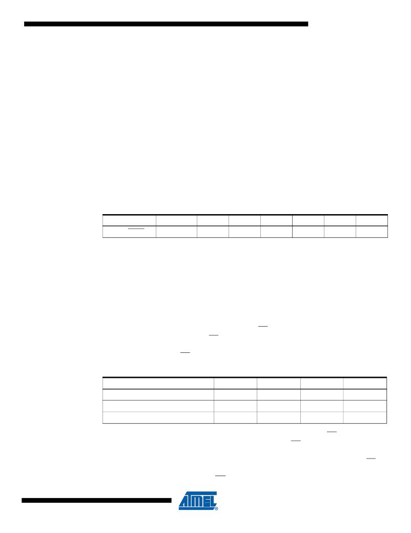
�Table� 5-2.�
�Status� Register� Format�
�Bit� 7�
�RDY/BUSY�
�Bit� 6�
�COMP�
�Bit� 5�
�1�
�Bit� 4�
�1�
�Bit� 3�
�0�
�Bit� 2�
�1�
�Bit� 1�
�Protect�
�Bit� 0�
�X�
�6.� Sector� Protection�
�Two� protection� methods,� hardware� and� software� controlled,� are� provided.� The� selection� of� which�
�sectors� to� be� protected/unprotected� from� program� and� erase� operations� is� defined� in� the� Sector�
�Protection� Register.�
�6.1�
�Software� Sector� Protection�
�Sectors� specified� for� protection� in� the� Sector� Protection� Register� can� be� protected� from� program�
�and� erase� operations� by� issuing� the� Enable� Sector� Protection� command.� To� enable� the� sector�
�protection� using� the� software� controlled� method,� the� CS� pin� must� first� be� asserted� as� it� would� be�
�with� any� other� command.� Once� the� CS� pin� has� been� asserted,� the� appropriate� 4-byte� command�
�sequence� must� be� clocked� in� via� the� input� pin� (SI).� After� the� last� bit� of� the� command� sequence�
�has� been� clocked� in,� the� CS� pin� must� be� deasserted� after� which� the� sector� protection� will� be�
�enabled.�
�Command�
�Enable� Sector� Protection�
�Disable� Sector� Protection�
�Read� Sector� Protection� Register�
�Byte� 1�
�3DH�
�3DH�
�32H�
�Byte� 2�
�2AH�
�2AH�
�00H�
�Byte� 3�
�7FH�
�7FH�
�00H�
�Byte� 4�
�A9H�
�9AH�
�00H�
�To� disable� the� sector� protection� using� the� software� controlled� method,� the� CS� pin� must� first� be�
�asserted� as� it� would� be� with� any� other� command.� Once� the� CS� pin� has� been� asserted,� the�
�appropriate� 4-byte� sequence� for� the� Disable� Sector� Protection� command� must� be� clocked� in� via�
�the� input� pin� (SI).� After� the� last� bit� of� the� command� sequence� has� been� clocked� in,� the� CS� pin�
�must� be� deasserted� after� which� the� sector� protection� will� be� disabled.� The� Disable� Sector� Pro-�
�tection� command� is� ignored� while� the� WP� pin� is� asserted.�
�9�
�3387M–DFLASH–2/08�
�发布紧急采购,3分钟左右您将得到回复。
相关PDF资料
AT45DB642-TC
IC FLASH 64MBIT 20MHZ 40TSOP
AT88CK9000-8TH
CRYPTO PROGRAMMER BOARD 8-TSSOP
AT88SC12816C-MJ
IC EEPROM 128KBIT 1.5MHZ M2J
AT88SC25616C-MJ
IC EEPROM 256BIT 1.5MHZ M2J
AT88SC3216C-MJ
IC EEPROM 32KBIT 1.5MHZ M2J
AT88SC6416C-MJ
IC EEPROM 64KBIT 1.5MHZ M2J
AT91EB40A
KIT EVAL FOR ARM AT91R40008
AT91EB42
KIT EVAL FOR ARM AT91M42800A
相关代理商/技术参数
AT45DB321C-TI
制造商:ATMEL 制造商全称:ATMEL Corporation 功能描述:32-megabit 2.7 volt DataFlash
AT45DB321C-TU
功能描述:IC FLASH 32MBIT 40MHZ 28TSOP RoHS:是 类别:集成电路 (IC) >> 存储器 系列:- 标准包装:1 系列:- 格式 - 存储器:RAM 存储器类型:SDRAM 存储容量:256M(8Mx32) 速度:143MHz 接口:并联 电源电压:3 V ~ 3.6 V 工作温度:-40°C ~ 85°C 封装/外壳:90-VFBGA 供应商设备封装:90-VFBGA(8x13) 包装:托盘 其它名称:Q2841869
AT45DB321D
制造商:ATMEL 制造商全称:ATMEL Corporation 功能描述:2.7V 32Mbit dataflash
AT45DB321D_07
制造商:ATMEL 制造商全称:ATMEL Corporation 功能描述:32-megabit 2.7-volt DataFlash
AT45DB321D_08
制造商:ATMEL 制造商全称:ATMEL Corporation 功能描述:32-megabit 2.7-volt DataFlash
AT45DB321D_09
制造商:ATMEL 制造商全称:ATMEL Corporation 功能描述:32-megabit 2.7-volt DataFlash
AT45DB321D_12
制造商:AD 制造商全称:Analog Devices 功能描述:32Mb, 2.5V or 2.7V DataFlash
AT45DB321D-CCU
功能描述:闪存 32M 2.7-3.6V, 66Mhz Serial 闪存 RoHS:否 制造商:ON Semiconductor 数据总线宽度:1 bit 存储类型:Flash 存储容量:2 MB 结构:256 K x 8 定时类型: 接口类型:SPI 访问时间: 电源电压-最大:3.6 V 电源电压-最小:2.3 V 最大工作电流:15 mA 工作温度:- 40 C to + 85 C 安装风格:SMD/SMT 封装 / 箱体: 封装:Reel